
2022-05-10
Circuit board, circuit board, PCB board, PCB welding technology in recent years, the development of electronic industry process, we can notice a very obvious trend is reflow technology. In principle, traditional inserts can also be reflow welded, which is commonly referred to as through-hole reflow welding. Its advantage is that it is possible to complete all welding joints at the same time, so that the production cost is minimized. However, temperature sensitive components limit the application of reflow soldering, whether it is inserts or smd Then people turn their attention to welding. In most applications, selective welding can be used after reflow welding. This will become an economical and effective welding method to complete the remaining inserts, and is fully compatible with future lead-free welding.

Principle of process technology
BGA welding adopts the principle of reflow welding. Here is the reflow mechanism of tin balls in the welding process.
When the tin ball is in a heated environment, the tin ball reflux is divided into three stages:
preheat
First, the solvent used to achieve the required viscosity and screen printing performance begins to evaporate, and the temperature rise must be slow (about 5 ° C per second) to limit boiling and splashing and prevent the formation of small tin beads. In addition, some components are sensitive to internal stress, and if the external temperature of the components rises too fast, it will cause fracture.
When the flux (paste) is active and the chemical cleaning action begins, the water-soluble flux (paste) and the non cleaning flux (paste) will have the same cleaning action, but the temperature is slightly different. Remove metal oxides and some contamination from the metal and solder particles to be bonded. Good metallurgical solder joints require "clean" surfaces.
When the temperature continues to rise, the solder particles first melt alone and begin the process of liquefaction and surface absorption of tin. This covers all possible surfaces and begins to form solder joints.
backflow
This stage is the most important. When all the individual solder particles melt, they combine to form liquid tin. At this time, the surface tension begins to form the surface of the solder pin. If the gap between the component pin and the PCB pad exceeds 4mil (1mil= one thousandth of an inch), it is very likely that the pin and the pad will be separated due to the surface tension, which will cause the open circuit of the tin dot.
cooling
In the cooling stage, if the cooling is fast, the tin dot strength will be slightly larger, but not too fast, otherwise it will cause temperature stress inside the element.
Process method
Before welding BGA, both PCB and BGA should be baked in a constant temperature oven at 80 ℃ ~ 90 ℃ for 10 ~ 20 hours in order to remove moisture and adjust the baking temperature and time appropriately according to the degree of moisture. PCB and BGA without unpacking can be welded directly. In particular, when carrying out all the following operations, you should wear electrostatic rings or anti-static gloves to avoid possible damage to the chip caused by static electricity. Before welding BGA, the BGA should be accurately aligned on the pad on the PCB. There are two methods: optical alignment and manual alignment. At present, manual alignment is mainly used, that is, the four sides of BGA are aligned with the silk screen lines around the pad on PCB. Here is a trick: in the process of aligning BGA with the silk screen line, even if it is not completely aligned, even if the tin ball and pad deviate by about 30%, it can still be welded. Because the tin ball will automatically align with the pad due to the tension between it and the pad during the melting process. After finishing the alignment operation, place the PCB on the bracket of BGA repair workstation and fix it so that it is level with BGA repair workstation. Select the appropriate hot air nozzle (that is, the nozzle size is slightly larger than the BGA size), then select the corresponding temperature curve, start welding, and finish BGA welding after the temperature curve is completed and cooled.
During production and commissioning, it is inevitable to replace BGA due to BGA damage or other reasons. BGA repair workstation can also complete the disassembly of BGA. Disassembly of BGA can be regarded as the reverse process of BGA welding. The difference is that after the temperature curve is completed, BGA should be sucked away with a vacuum suction pen. The reason why other tools, such as tweezers, are not used is to avoid damaging the pad due to excessive force. Remove the tin from the PCB with BGA removed while it is hot (remove the tin on the pad). Why do you want to operate while it is hot? Because the hot PCB is equivalent to the preheating function, it can ensure that the tin removal work is easier. Here we need to use a tin suction line. Don't use too much force during the operation to avoid damaging the pad. After ensuring that the pad on the PCB is flat, we can weld BGA.
Can the removed BGA be welded again? The answer is yes. But before that, there is a key step, that is, planting the ball. The purpose of ball planting is to replant the tin ball on the bonding pad of BGA, which can achieve the same arrangement effect as the new BGA. Here is a detailed introduction to the next planting ball. Here we need to use two tools, steel mesh and tin suction wire.
Remove tin slag
First of all, we need to remove the excess tin slag on the BGA. The requirement is to make the BGA surface smooth without any burrs (formed by tin).
Step 1 - apply welding paste (flux)
Place BGA on the conductive pad and apply a small amount of welding paste (flux) on the surface of BGA.
Step 2 - remove the tin ball
Remove the tin ball from BGA with tin suction wire and soldering iron. Place the tin absorption line on the soldering paste and put the soldering iron on the tin absorption line
Before you scratch the tin washing line on the BGA surface, let the soldering iron heat the tin suction line and melt the tin ball.
Note: do not let the soldering iron press on the surface. Excessive pressure will cause cracks on the surface to scrape off the pad. In order to achieve the best effect, it is best to use the tin absorption wire to pass through the BGA surface at one time. A small amount of solder paste left on the pad will make it easier to plant the ball.
Step 3 - cleaning
Immediately clean the BGA surface with industrial alcohol (plate washing water). At this time, timely cleaning can make it easier to remove the residual welding paste.
Remove the welding paste on the BGA surface by friction movement. Maintain mobile cleaning. When cleaning, always start from the edge and don't forget the corner.
Clean solvent shall be used when cleaning each BGA
Step 4 - Inspection
It is recommended to examine under a microscope. Observe clean pads, damaged pads and solder balls that have not been removed.
Note: due to the corrosivity of the flux, it is recommended to carry out additional cleaning if the ball planting is not carried out immediately.
Step 5 - excessive cleaning
Scrub the BGA surface with deionized water and a brush.
Note: in order to achieve the best cleaning effect, use a brush to wash back and forth from one direction to one corner of the packaging surface. Cycle scrubbing.
Step 6 - flushing
Rinse the BGA surface with deionized water and a brush. This helps remove the residual solder paste from the BGA surface.
Next let BGA dry in the air. Use step 4 to repeatedly check the BGA surface.
If BGA is placed for a period of time before ball planting, it can basically ensure that they are very clean. It is not recommended to soak BGA in water for too long.
After the above operations, you can plant the ball. Steel mesh and planting platform are used here.
Planting ball
The function of steel mesh is to easily place tin balls on the corresponding pads of BGA. The function of the ball planting table is to melt the tin ball on BGA and fix it on the pad. When planting balls, first apply a layer of welding paste (flux) evenly on the BGA surface (the side with bonding pad), and the amount of application should be no more than a little. More or less application may cause failure of ball planting. Align each hole on the steel mesh (universal steel mesh is used here) with each pad on BGA. Then pour the tin balls onto the steel mesh, use a brush or other tools to pull the tin balls into each hole of the steel mesh, and the tin balls will reach the bonding pad of BGA along the hole. After this step, carefully check whether there is a tin ball that is not aligned with the pad. If so, use a needle to correct it. Carefully remove the steel mesh, put the BGA on the high-temperature paper and put it on the ball planting table. The temperature setting of the ball planting table is based on the lead tin ball 220 ℃ and the lead-free tin ball 235 ℃. The planting time is not fixed. In fact, it is judged by the fact that the tin balls on BGA are melted and the surface is shiny, forming a complete ball. These are observed by the naked eye. You can record the time it takes to reach this state, and the next planting can be carried out according to this time.
BGA ball planting is a work that requires patience and care. It is necessary to be careful when operating
Be careful.
1.3 current domestic and international level
BGA (ballgridarraypackage) is the most popular packaging form in recent years
Its appearance can greatly improve the integration and manufacturability of chips. Because China is
BGA welding technology started late, and domestic manufacturers can manufacture BGA repair workstations
There are not many homes, so there are few BGA repair workstations in China, especially in the West.
With optical alignment, BGA repair stations with X-ray function are more rare. Maybe China can establish more repair stations in X-ray in the later stage. At present, Yinghua test provides this aspect of testing in the eastern part. Let's look at the technical aspect!
1.4 technical difficulties solved
In actual work, we will encounter different sizes and thicknesses of PC
Small BGAs are lead-free and lead-free. They also use different temperature curves. Therefore, it is impossible to weld all BGAs with one temperature curve. How to set different temperature curves according to different conditions is the key in BGA welding process. Here are several groups of pictures to illustrate.
There are many reasons for the wrong temperature. Another reason is that the temperature curve is tested in an air-conditioned environment, that is, it is not normal temperature. In summer and winter, the temperature of the air conditioner is inconsistent with the normal temperature, so it will be higher or lower when setting the BGA temperature curve. Therefore, when welding each time, it is necessary to test whether the actual temperature conforms to the set temperature value. The principle of temperature setting is to first set the corresponding temperature according to the lead-free welding or lead-free welding, then test the actual temperature with a thermometer (or thermocouple), and then adjust the set temperature according to the actual temperature to achieve the most ideal temperature for welding. In the process of welding, it must be ensured that the BGA repair workstation, PCB and BGA are on the same level, and vibration cannot occur during the welding process, otherwise bridging will occur when the tin ball melts, causing a short circuit.
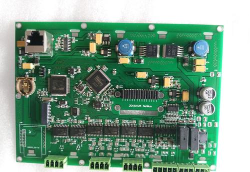
The design of PCB board is generally good. The board not only saves materials, but also has good electrical characteristics in all aspects, such as heat dissipation, anti-interference, etc.
quality testing
At present, the inspection methods of circuit board welding quality include visual inspection, infrared detection, online testing, etc. Among these methods, the most economical and commonly used is the visual method, which is economical, convenient, simple and feasible. Other methods need some equipment support. Although they invest a lot, they can ensure high inspection reliability.
1. Visual method
The visual method directly observes the welding condition on the surface of the solder joint by human eyes, and can check the welding defects such as poor wettability, inappropriate solder quantity, solder pad falling off, bridging, small solder ball splashing, Matt solder joint and solder leakage. The simplest tool for visual method is a magnifying glass, which generally uses a fixed magnifying glass with a lamp of 5-10 times. It is completely applicable to the inspection of circuit board welding with low density. The disadvantage of this tool is that inspectors are prone to fatigue, and the better visual inspection instrument is the camera screen display inspection instrument, whose magnification is adjustable, up to 80-90 times. It displays the welding part of the board on the screen through CCD, and people can observe the screen like watching TV. The higher-grade tester can automatically move the circuit board welding in two directions, and can also automatically position, so as to realize the inspection of the key parts of PCBA. Equipped with a video recorder, the inspection results can be recorded.
2. Infrared detection method
The infrared detection method uses the infrared beam to radiate heat to the welding spot of the circuit board, and then detects whether the heat release curve of the welding spot is normal, so as to judge whether there is a hole in the welding spot, so as to achieve the purpose of indirectly checking the welding quality. This inspection method is suitable for large quantities of automatic welding, with good pad consistency and little difference in the volume of components. Otherwise, other factors have too much influence on the heat dissipation characteristics of the solder joint The false detection rate will increase. Because this method is subject to many restrictions, after all, the solder joint size of any kind of circuit board welding will be different. Therefore, it is less used in the detection of electronic products.
3. X-ray fluoroscopy
X-ray fluoroscopy shows the density distribution of welding thickness, shape and quality by taking advantage of the fact that the ability of X-ray to pass through solder is not as strong as that of copper, silicon, FR-4 and other materials. This detection method is applicable to invisible solder joints (i.e. hidden welding). It places the circuit board to be tested in the X-ray channel, and it can be seen on the display screen that the solder joint solder prevents the X-ray from passing through the formed solder joint contour.
4. Online testing method
The on-line test method is realized by the on-line tester, which connects the test points on the circuit board welding with the tester through the signal connecting part called "needle bed" on the tester. It can check the open circuit, short circuit and fault components welded on the circuit board, as well as the functions of components, such as the value of resistance and capacitance, the polarity of transistors, etc. Through the floating pin test method of IC, the faulty soldering pin of IC can be checked. If the density of components on the circuit board is high and it is difficult to set the required test points, the boundary scanning technology can be used to collect those test points to the edge connector welded on the circuit board through the designed test circuit, so that the on-line tester can measure the required points at various positions.
Online test method is an electrical signal test method. It can check the welding state of circuit board welding, which is very close to the practical situation. Generally, the circuit board welding that has passed the online test can be installed and used, but it cannot give the quality results of welding, and it does not visually check the reliability of welding joints.

